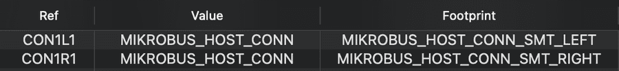
KiCAD Footprints with Multiple Parts for PCBA
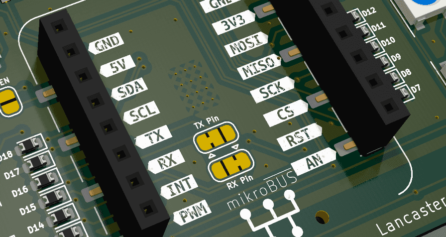
The process begins with an original component that consists of two physically independent connectors housed in a single package. This is a common scenario with certain types of board-to-board connectors or specialized interface headers where manufacturing constraints require separate physical components, but the electrical design treats them as a unified part.
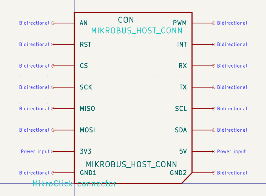
To start the modification process, open the symbol in KiCAD’s symbol editor. Create two duplicate copies of this original symbol - one designated as the ‘left’ variant and another as the ‘right’ variant. The terms ‘left’ and ‘right’ here should be adjusted to match the actual geometry of your specific part, or whatever logical separation makes sense for your design. The key is establishing a clear distinction between the two physical components.
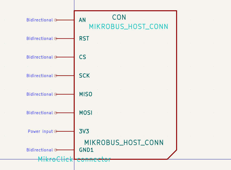
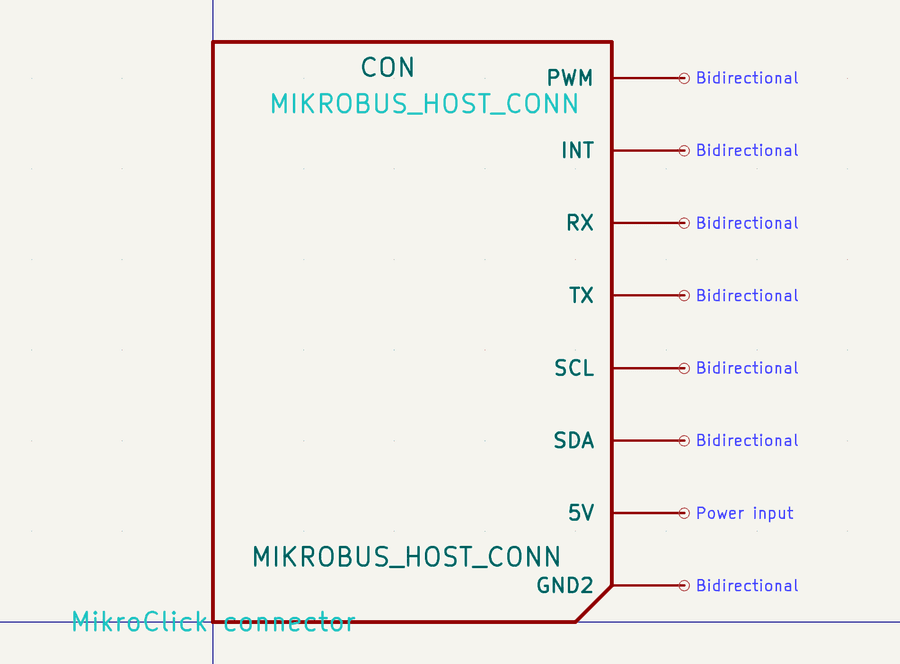
Once you have your duplicated symbols, begin editing the left variant by carefully deleting all the connector pins that correspond to the right physical connector. This is where attention to detail becomes critical: you must preserve the original pin numbers during this deletion process. The pin numbering must remain consistent with the original part datasheet, as this maintains the electrical connections when you eventually place both parts on your PCB. Repeat this process in reverse for the right symbol variant, removing all the left connector pins while again preserving the pin numbers.
With the symbols prepared, transition to KiCAD’s footprint editor and locate the corresponding footprint for your part. In my case, I started with a standard through-hole variant, but found it necessary to create a custom surface-mount variant using offset pin headers to meet the assembly requirements. The specific mounting style you choose will depend on your manufacturing process and board design constraints.
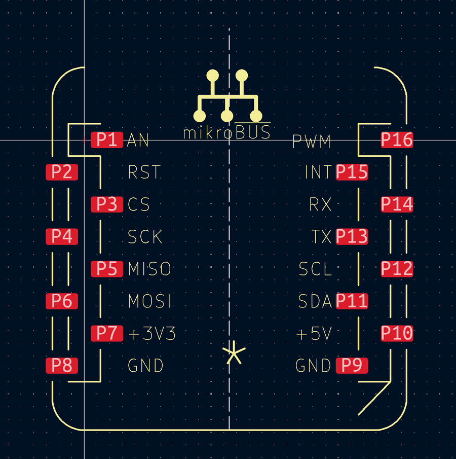
The next crucial step involves establishing a clear division line on the footprint. Draw a ‘cut’ line that defines where the part will be split - I recommend using the F.fab layer for this purpose, as it’s intended for fabrication documentation. Critically, ensure this cut line is aligned to the editor grid, as this alignment will make reassembly in the PCB layout much cleaner and prevent any potential alignment issues during placement.
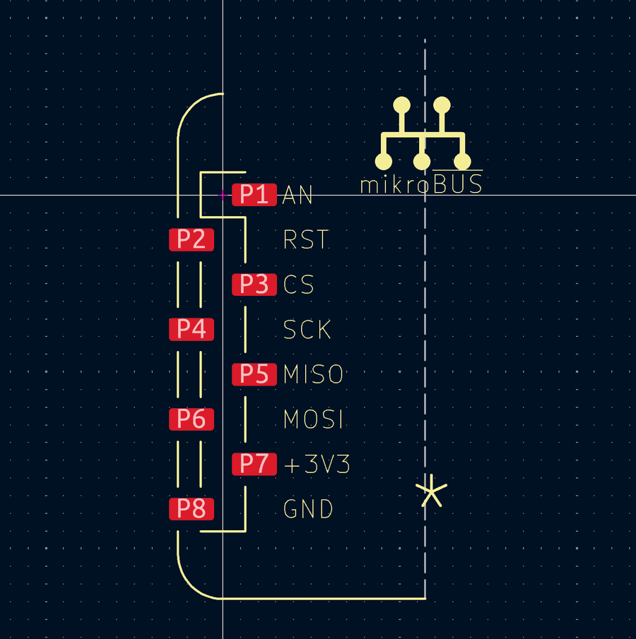
Following the same pattern used with the symbols, duplicate the footprint twice to create left and right variants corresponding to each physical component. On the left footprint, methodically remove all elements on the right side of your cut line - this includes pads, mounting holes, silkscreen markings, and any other footprint features. Then perform the inverse operation on the right footprint, removing all left-side elements. The result should be two footprints that, when placed together, perfectly reconstruct the original part geometry.
Return to your PCB layout editor where the payoff becomes apparent. Place both the left and right footprint variants on your board, carefully aligning them along the cut line you established earlier. When properly aligned, they should seamlessly rebuild the complete part as if it were never split. This alignment is why the grid-snapping during the cut line creation was so important.
The final benefit of this approach shows in your Bill of Materials. Instead of a single entry for the composite part, you now have two BOM entries. This separation allows you to specify two distinct physical parts for placement, which is exactly what PCBA (Printed Circuit Board Assembly) services require. This resolves the fundamental 1:1 part mapping issue where assembly systems expect each footprint to correspond to exactly one physical component, avoiding the confusion and potential errors that arise when a single BOM entry needs to map to multiple placement locations.